High-Density Interconnect PCB
An HDI PCB (High-Density Interconnect PCB) stands out with significantly greater wiring density compared to traditional through-hole PCBs. As specified in IPC-6012, it is characterised by an average of at least 20 electrical connections per square centimetre on both sides of the board, enabling compact and complex designs.
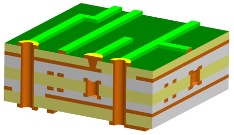
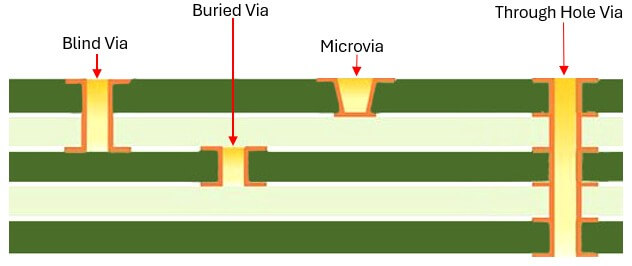
HDI boards are commonly used to achieve smaller, lighter, more powerful and reliable electronic devices by utilising multiple layers, fine tracks and gaps, microvias, and blind and buried vias. With HDI a shorter signal path ensures power loss is less, and therefore its overall electrical performance is better which supports high-speed signals and improved signal integrity which is essential many cutting-edge technology products.

HDI PCBs (High-Density Interconnect Printed Circuit Board)should follow IPC2226, the standard for design such PCBs including features such as:

| Feature | Technical Specification |
|---|---|
| Max layer count | 22, advanced 50 |
| PCB thickness | 0.3mm - 4.5mm |
| PCB size | 50 x 50mm - 700 x 600mm |
| Max copper thickness | Outer layer:6OZ Inner layer: 6OZ |
| Minimum hole size | 0.1mm, advanced 0.075MM |
| Max hole size | 3.5mm |
| Tighest hole tolerence | PTH:±0.075MM, NPTH:±0.05MM |
| Min track width | 0.762mm |
| Min gap | 0.762mm |
| Finishes | OSP, ENIG, ENEPIG, EPAG, Immersion tin, Immersion Silver |